9 EUV Photoresists Market Growth Accelerated by Advanced Semiconductor Manufacturing
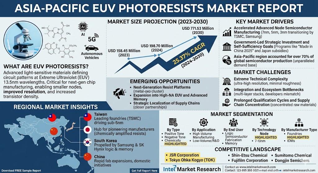
According to a new report from Intel Market Research, the Asia-Pacific EUV Photoresists market was valued at USD 158.45 million in 2023 and is projected to grow from USD 198.70 million in 2024 to USD 771.53 million by 2030, exhibiting a robust CAGR of 25.37% during the forecast period (2024–2030). This growth is propelled by the expansion of leading semiconductor foundries like TSMC in Taiwan and Samsung in South Korea, surging demand for advanced nodes below 7nm, substantial government investments in Japan, China, and the region, and the growing adoption of EUV lithography for high-volume manufacturing.
What are EUV Photoresists?
EUV Photoresists are advanced light-sensitive materials used in semiconductor lithography to define circuit patterns with extreme precision at extreme ultraviolet (EUV) wavelengths of 13.5nm. These materials play a critical role in next-generation chip manufacturing, enabling smaller node sizes, improved resolution, and increased transistor density. They are essential for producing high-performance microchips in cutting-edge applications such as artificial intelligence, 5G, and autonomous vehicles.
This report provides a deep insight into the Asia-Pacific EUV Photoresists market covering all its essential aspects-from a macro overview of the market to micro details such as market size, competitive landscape, development trends, niche markets, key drivers and challenges, SWOT analysis, and value chain analysis.
📥 Download FREE Sample Report: Asia-Pacific EUV Photoresists Market - View in Detailed Research Report
The analysis helps the reader understand competition within the industry and strategies for enhancing profitability. Furthermore, it provides a framework for evaluating and accessing the position of a business organization. The report also focuses on the competitive landscape of the Asia-Pacific EUV Photoresists Market, introducing market share, performance, product positioning, and operational insights of major players. This helps industry professionals identify key competitors and understand the competition pattern.
In short, this report is a must-read for industry players, investors, researchers, consultants, business strategists, and all those planning to foray into the EUV Photoresists market.
Key Market Drivers
1. Accelerated Advanced Node Semiconductor Manufacturing
The relentless pursuit of miniaturization in semiconductor fabrication is the principal driver for the Asia-Pacific EUV photoresists market. Leading foundries and memory manufacturers in South Korea, Taiwan, and increasingly Japan and China are transitioning to 7nm, 5nm, and 3nm process nodes. At these dimensions, traditional 193nm immersion lithography reaches its physical limits, making EUV lithography the only viable patterning technology. This technological imperative is creating a significant and sustained demand for advanced photoresists specifically engineered for 13.5nm wavelength exposure, essential for producing the next generation of logic chips and high-density memory.
2. Government-Led Strategic Investment and Self-Sufficiency Goals
National policies across the region are providing a powerful stimulus for market growth. Governments recognize semiconductors as critical infrastructure and are implementing substantial financial and policy support. Programs like China's "Made in China 2025" initiative and Japan's subsidies for domestic semiconductor resurgence are funneling billions of dollars into fab construction and R&D, which directly includes the development and procurement of advanced materials like EUV photoresists. This state-backed investment aims to secure the supply chain and reduce external dependencies, fostering a robust local ecosystem for the Asia-Pacific EUV photoresists market.
➤ The Asia-Pacific region accounted for over 70% of global semiconductor device production in the past year, establishing an unparalleled demand base for lithography materials essential for maintaining this manufacturing leadership against rising global competition.
Concurrently, the explosion of data-centric technologies, including 5G infrastructure, artificial intelligence, and high-performance computing, is fueling the need for more powerful and efficient chips. These end-use applications require the advanced node capabilities enabled by EUV lithography, thereby creating a pull-through effect on the entire ecosystem, including the critical photoresist materials.
Market Challenges
- Extreme Technical Complexity and Stringent Performance Requirements – The formulation and production of EUV photoresists represent one of the most challenging material science hurdles in the semiconductor industry. These photoresists must exhibit ultra-high resolution, exceptional sensitivity to low-dose EUV light, and minimal line-edge roughness to achieve precise patterning.
- Integration and Ecosystem Bottlenecks – Successful implementation extends beyond the photoresist material itself. Challenges remain in its integration with complex multi-layer stack schemes, underlayers, and developers. Any mismatch can lead to defectivity and yield loss.
- Prolonged Qualification Cycles and Supply Chain Concentration – A new EUV photoresist formulation must undergo years of testing on actual production wafers. Additionally, the supply chain for key raw materials is highly concentrated, creating potential vulnerabilities and pricing pressures.
Emerging Opportunities
The Asia-Pacific semiconductor landscape is becoming increasingly favorable for advanced materials development and commercialization. Growing strategic investments, supportive policy frameworks, and industry collaborations are accelerating market expansion. Key growth enablers include:
- Development of next-generation resist platforms such as metal-oxo cluster-based photoresists promising higher EUV absorption and etch resistance.
- Expansion into High-NA EUV and specialty applications for advanced memory patterning and photomask production.
- Strategic localization of supply chains for closer partnerships with domestic foundries and IDMs.
Collectively, these factors are expected to enhance innovation, stimulate adoption, and drive EUV photoresists’ penetration across advanced nodes and applications.
📥 Download Sample PDF: https://www.intelmarketresearch.com/download-free-sample/41329/asia-pacific-euv-photoresists-market-market
Regional Market Insights
- Taiwan: Taiwan stands at the forefront, driven by leading foundries like TSMC heavily relying on EUV lithography for sub-5nm node production, fostering close collaborations and innovations in high-sensitivity photoresists.
- Japan: Japan excels as the hub for pioneering manufacturers developing chemically amplified resists with exceptional resolution, supporting regional supply chains through technical collaborations.
- South Korea: South Korea is propelled by Samsung and SK Hynix advancing logic and memory technologies, with heavy investments driving demand for high etch selectivity materials.
- China: China’s rapid ascent features aggressive fab expansions and domestic development initiatives prioritizing high-sensitivity EUV materials for self-sufficiency.
- Rest of Asia-Pacific: Emerging markets like India and Southeast Asia show promising growth through infrastructure investments and technology transfer.
Market Segmentation
Segment Analysis:
|
Segment Category |
Sub-Segments |
Key Insights |
|
By Type |
|
Chemically Amplified EUV Photoresists
|
|
By Application |
|
High-Volume Manufacturing (HVM)
|
|
By End User |
|
Logic Semiconductor Fabrication
|
|
By Technology Node |
|
< 7 nm Technology
|
|
By Manufacturer Type |
|
Foundries
|
📘 Get Full Report Here: Asia-Pacific EUV Photoresists Market - View Detailed Research Report
Competitive Landscape
Japanese firms like JSR Corporation and Tokyo Ohka Kogyo Co., Ltd. (TOK) dominate the current market, holding the largest shares due to their pioneering roles in high-sensitivity, low-roughness materials.
The report provides in-depth competitive profiling of 14+ key players, including:
- JSR Corporation
- Tokyo Ohka Kogyo Co., Ltd. (TOK)
- Shin-Etsu Chemical Co., Ltd.
- Fujifilm Corporation
- Sumitomo Chemical Co., Ltd.
- Dongjin Semichem Co., Ltd.
- Others including Fujifilm Electronic Materials, JSR Micro, Inc., and Nippon Kayaku Co., Ltd.
Report Deliverables
- Asia-Pacific market forecasts from 2024 to 2030
- Strategic insights into R&D developments, technology trends, and supply chain dynamics
- Market share analysis and SWOT assessments
- Trends in advanced nodes and material innovations
- Comprehensive segmentation by type, application, end user, technology node, and manufacturer type
📘 Get Full Report Here: Asia-Pacific EUV Photoresists Market - View Detailed Research Report
📥 Download FREE Sample Report:
Asia-Pacific EUV Photoresists Market - View in Detailed Research Report
About Intel Market Research
Intel Market Research is a leading provider of strategic intelligence, offering actionable insights in biotechnology, pharmaceuticals, and healthcare infrastructure. Our research capabilities include:
- Real-time competitive benchmarking
- Global clinical trial pipeline monitoring
- Country-specific regulatory and pricing analysis
- Over 500+ healthcare reports annually
Trusted by Fortune 500 companies, our insights empower decision-makers to drive innovation with confidence.
🌐 Website: https://www.intelmarketresearch.com
📞 Asia-Pacific: +91 9169164321
🔗 LinkedIn: Follow Us